
Inspection Setup Principle
There is no single “best” magnification for every PCB inspection task. Approximately 5×–30× is a useful reference range for many general stereo or digital microscope inspections, but it is not a universal setting or a figure that can be compared directly with every video microscope’s screen magnification. A view that reveals a fine solder bridge may be too narrow for moving efficiently across the assembly. The practical choice depends on whether the defect can be judged, how much of the surrounding PCB remains visible and whether components and tools fit beneath the optics at the focused position.
The image needs enough optical detail to separate an acceptable condition from the defect the inspection is intended to catch.
A wider field of view preserves board landmarks and reduces the time spent searching, repositioning and recovering the target.
The focused position must leave room for components, fixtures and any tool that needs to enter the inspection area.
Start With the Inspection Decision, Not the Maximum Magnification
A technician scanning a populated PCBA needs to recognize connectors and component groups quickly. The same technician may then need a much closer view to distinguish a suspect solder bridge or examine a fine crack. One fixed, high setting rarely handles both jobs well: it may show the detail, but leave too little of the board visible to find the next inspection point.
The useful starting point is the smallest visible feature that could change an accept/reject decision. But the neighboring pads, leads or component edges may be just as important for interpreting what is on screen. Once that detail is clear, record the actual field-of-view width in millimeters. It gives operators and suppliers a practical reference for comparing microscopes without treating a large magnification figure as proof of a better inspection.
At this stage, seeing an entire connector or IC neighborhood is often more useful than seeing individual solder grains. The operator needs to know where the next check begins.
Useful field of view and fast target acquisition.
A joint can look convincing in isolation yet be difficult to judge without its adjacent pad or lead. The view should show enough detail for the criterion and enough context to interpret it.
Enough resolved detail for a repeatable decision.
A suspected crack or particle may call for a closer look, particularly when the normal view leaves doubt about its edge or extent. That closer view need not become the default.
More detail for confirmation, not routine navigation.
A supplier demonstration can look excellent while the board stays still. The more revealing test is what happens after the operator moves away from a solder joint: can they find the next location quickly, judge it with confidence and return to a familiar wider view?
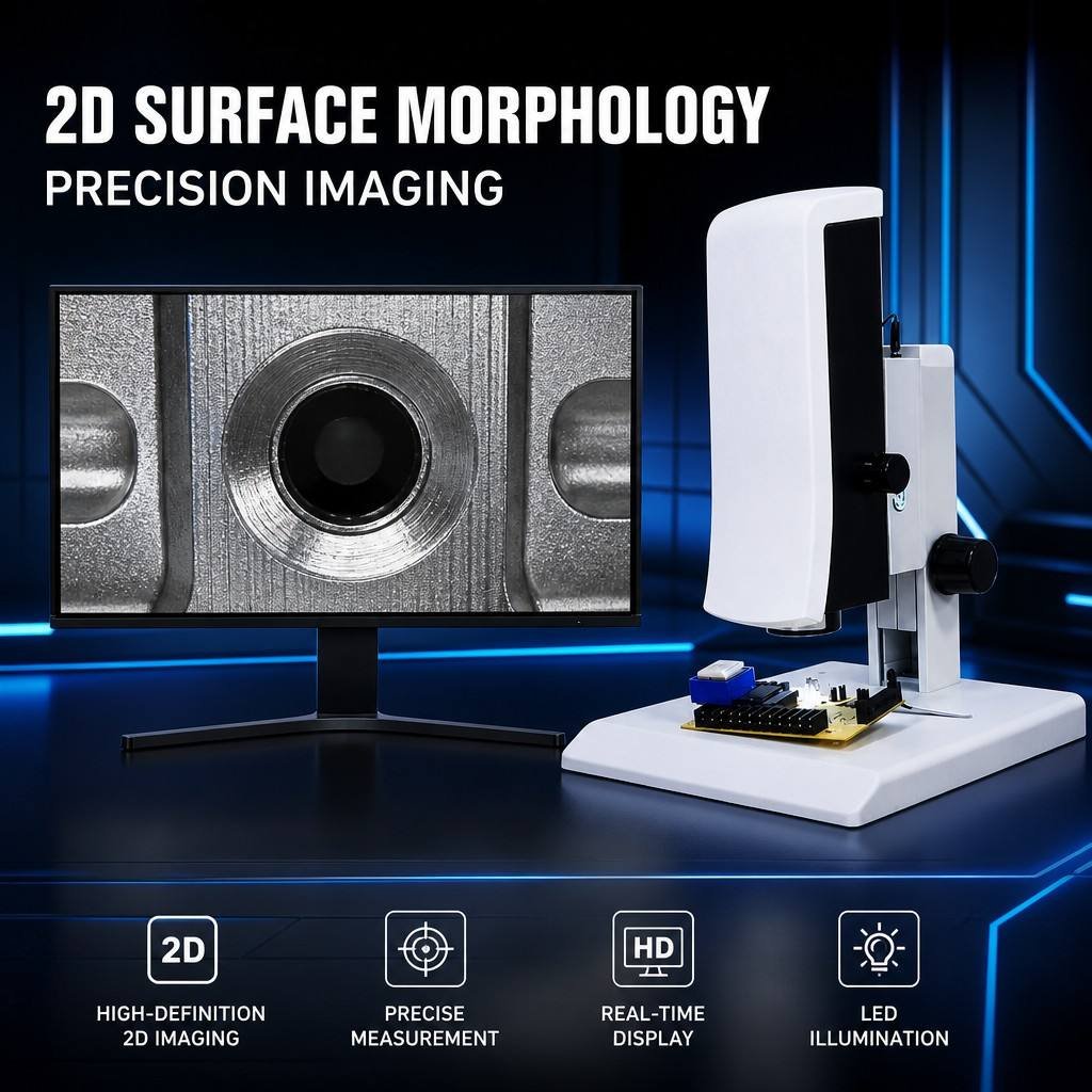
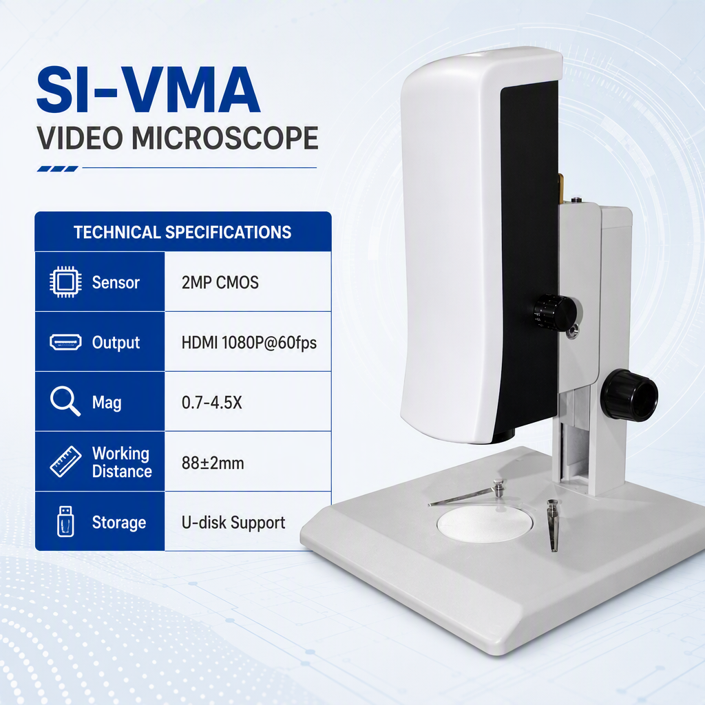
For an example of how these choices apply to a real system, compare PCB inspection magnification and working distance with the SI-VMA video microscope. The product details provide a starting point, but the useful field of view and tool clearance still need checking on your own board. If you are deciding which type of microscope to buy, our PCB quality-control microscope selection guide covers that broader decision.
What Changes as PCB Microscope Magnification Increases?
Higher magnification changes more than how large the component appears on screen. Within the same optical system, increasing optical magnification reduces the physical area visible at one time. Depth of field also generally becomes shallower as magnification increases, so mixed-height PCB assemblies can require more frequent focus adjustment.
Consider a fine-pitch IC surrounded by passives. A wider view lets the operator identify the package and the row of leads to inspect; a tighter view may show only a few leads at once. That extra detail helps when one joint looks questionable, but it slows routine inspection if the operator has to search for every location again. For context, Leica Microsystems’ PCB inspection guide discusses a practical 5×–30× range for general stereo and digital inspection; the optical configuration and field of view still need to be considered when comparing systems.
Becomes smaller as optical magnification rises, reducing the amount of board visible at once.
Typically becomes shallower, making height changes across packages and solder features more significant.
Can decrease when the operator spends more time repositioning, refocusing or recovering lost board landmarks.
Optical magnification and digital magnification are not interchangeable
Optical magnification changes the scale of the image formed by the lens, but increasing magnification alone does not guarantee finer resolved detail. Digital magnification enlarges the image that has already been captured. Digital enlargement can make an existing feature easier to view on screen, but it cannot recover fine optical detail that was never resolved in the original image.
On an external monitor, software enlargement can make a feature appear substantial without showing any new detail. A useful demonstration therefore compares the smallest relevant defect at the intended viewing arrangement, not just the largest zoom number displayed on a product sheet.
Practical rule: use the lowest optical magnification that reliably resolves the inspection requirement. Increase magnification when it adds decision-relevant detail, not simply because additional zoom is available.
Lighting can determine whether extra magnification actually helps
Solder joints, metal shields, component markings and dark molded packages respond differently to illumination. A highly magnified image with glare over the critical edge may provide less usable information than a slightly wider image with controlled lighting. When the board includes reflective solder next to dark components, evaluate illumination and magnification together rather than treating them as separate specifications.
A flat printed target cannot show what happens when a solder fillet reflects light straight into the lens or a tall connector casts a shadow across a nearby pad. Those are the surfaces worth bringing to a demonstration.
Determine Microscope Working Distance From the Real Clearance Envelope
Microscope working distance is the clear distance from the front of the objective to the specimen plane when the sample is in focus. For PCB work, however, the practical question is not simply whether a board fits under the microscope. The entire operating envelope has to fit while the image remains focused.
On a populated board, a connector or heat sink near the inspection point may extend toward the optical head even when the joint itself is in focus. Board holders and clamps affect how the assembly sits in the stand, while a ring light or other accessory can narrow the space around the objective.
Tool access matters just as much. A probe or soldering iron usually approaches at an angle and needs room to move beside neighboring components. A flat test board can therefore pass a focus check while the real assembly prevents the operator from reaching the joint comfortably.
Stand travel should not be confused with optical working distance. A stand may move the optical head high enough to physically clear a board, but the selected objective still has to focus at that position. The relevant specification is the usable working distance at focus for the actual lens configuration. Fixture height affects where the board sits within the stand, but should not simply be added to the optical working-distance specification.
How to test microscope working distance with fixtures
Place a representative production board in the same holder or fixture used at the workstation. Move the tallest realistic component region beneath the optical axis, focus the microscope, and then introduce the real tool from its normal operating angle. Repeat the test at the board edges and around any fixture clamps that could limit access.
Do not perform this check using only an empty stage or a flat calibration card. That test confirms that the optical system can focus; it does not confirm that the production task is physically workable.
What the bench test reveals: a microscope can focus sharply on the board and still leave too little room to reach the joint. Record the limiting component, tool angle and usable clearance rather than relying on stand height alone.
Use a Low-, Medium- and High-Magnification Inspection Workflow
In a typical inspection pass, the zoom setting changes for a reason. A wide view takes the operator to the correct component group, a closer view shows whether the joint meets the required criterion, and a very tight view is reserved for the occasional edge or mark that is still uncertain. The point is not to use every available magnification, but to avoid letting the hardest defect dictate the view for the entire board.
Locate
Begin with a wider field of view. Use board landmarks, package outlines, connectors and neighboring components to reach the inspection area quickly.
Judge
Increase optical magnification only until the solder joint, lead, edge or defect can be evaluated consistently against the required inspection criteria.
Confirm
Use a tighter view when a suspected fine defect remains ambiguous. Once the decision is made, return to the wider view for the next location.
Consistency matters here as much as sharpness. If two inspectors need very different zoom positions to judge the same visible joint, the team may need to agree on the required detail and field of view. A repeatable decision view is more useful on a production bench than a maximum magnification figure nobody uses.
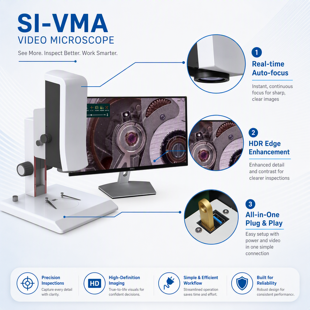
Autofocus can reduce the interruption caused by moving between features at different heights, but it does not remove the need to select an appropriate field of view. The SI-VMA product documentation lists Auto, One-Touch and Manual focus modes, allowing focus behavior to be matched to the inspection step rather than relying on one mode for every task.
The image may show the joint beautifully while hiding the neighboring pads that tell the operator exactly where they are.
A defect can fill the monitor and still lack the fine detail needed for a reliable judgment.
A bare test board may clear the lens easily; a connector, clamp or angled soldering tip can change the result.
A sharp image of a clean sample says little about glare on real solder or focus around uneven component heights.
Validate Magnification, Lighting and Working Distance on Representative PCBs
This is where a convincing demonstration can still fail the real job. A bright image of a clean PCB says little about a borderline solder defect hidden by glare or a connector that blocks the tool path. Testing a normal board alongside the most difficult representative samples exposes those limits before the workstation is approved.
A practical workstation validation sequence
- Find the target at a wide view Confirm that an operator can move from a known board landmark to the inspection point without excessive searching.
- Set the decision magnification Increase optical magnification until the critical feature becomes clear enough for a repeatable accept/reject decision.
- Test the smallest critical defect Use a known representative condition rather than judging sharpness from text, a ruler or an unrelated demonstration object.
- Challenge the lighting Inspect reflective solder, dark molding and shadowed regions to confirm that the illumination does not hide the relevant boundary.
- Insert fixtures and tools At the focused working position, confirm clearance around the highest component and through the actual tool approach path.
- Move away and return Repeat target recovery several times to judge how easily the workstation supports repeated production inspection.
The validation should also use the display arrangement planned for production. Screen size changes how large an image appears to the operator, while optical field of view remains an optical characteristic of the microscope setup. Avoid approving a workstation merely because a very large display makes the image look highly magnified.
Record the qualified inspection condition so purchasing and production are evaluating the same setup.
PCB / defect reference → optical zoom position → objective configuration → field of view → working distance → lighting condition → fixture / tool clearance → acceptance result
Two microscopes with very different advertised magnification figures can still be compared fairly if they show the same defect at a recorded field of view and leave enough room for the same fixture and tools. Those observations are more meaningful than a brochure comparison alone.
When This Type of System Is Worth Evaluating
Use the application test to decide whether the SI-VMA fits the workstation
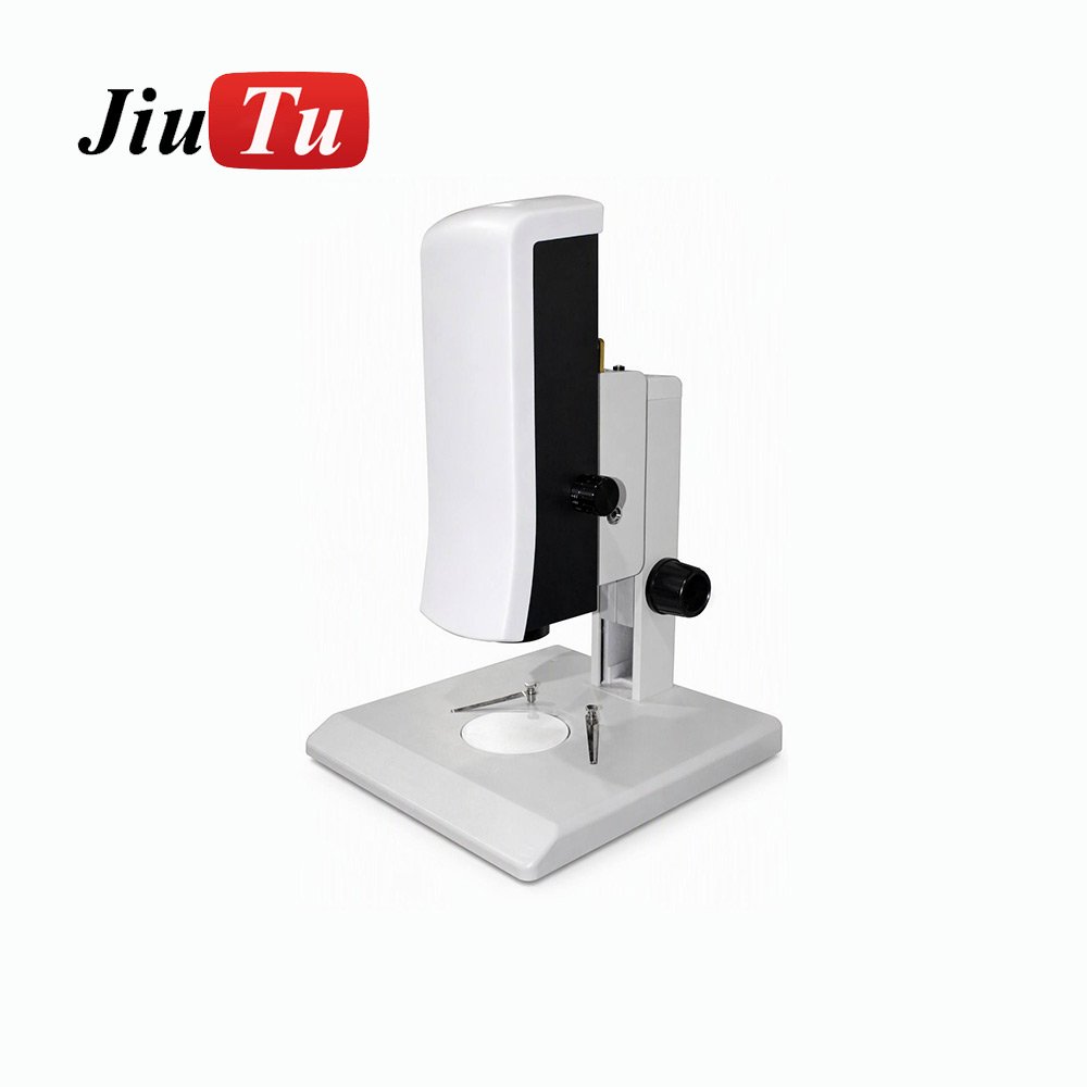
The SI-VMA becomes relevant when the inspection workflow benefits from screen-based viewing, adjustable optical magnification and focus control across components of different heights. Its product documentation specifies a manual 0.7–4.5X continuous zoom lens, additional electronic magnification, three focus modes, HDMI output, adjustable ring illumination and support for interchangeable objectives.
Autofocus and zoom are useful only if the proposed objective and stand still give the operator enough detail and working space on the real PCB. A configuration that looks capable on paper may need a different objective or mounting arrangement once the fixture is in place.
- Use a representative board rather than a generic sample.
- Include the highest component and normal fixture.
- Test the smallest critical defect used for inspection decisions.
- Bring the tool or probe that must operate under the lens.
- Confirm the field of view and usable working distance in the quoted configuration.
Frequently Asked Questions
Is higher magnification always better for PCB inspection?
No. Higher optical magnification can reveal smaller local features, but it also narrows the field of view and typically reduces depth of field. If the operator already has enough detail to make the inspection decision, increasing magnification further can make board navigation and repeated inspection slower without improving the decision.
What working distance is needed for soldering under a microscope?
There is no universal value. The required working distance depends on the tallest component, fixture height, soldering tool dimensions and the angle at which the tool approaches the joint. Verify clearance with the real board and tool while the microscope is focused, not with an empty stage.
How does field of view change with magnification?
Within the same optical configuration, field of view becomes smaller as optical magnification increases. That is why a wider setting is normally more efficient for locating a target, while a tighter setting is better reserved for detailed judgment or defect confirmation.
Should optical or digital magnification be prioritized?
Prioritize sufficient optical detail for the inspection decision. Digital magnification can enlarge an image that has already been captured, which may improve viewing comfort, but it cannot recreate optical detail that the lens and camera did not resolve.
Turn Magnification and Working Distance Into Acceptance Criteria
On a production bench, the best view is the one the operator can return to reliably. It shows the defect clearly without turning every movement across the board into a search, and it leaves room for the actual assembly and tools.
Before approving a configuration, give the supplier the board and a defect that genuinely matters to your QC process. Ask to see that defect at a useful field of view, then check what happens when the board is moved and the normal fixture or tool is introduced. The result is easier to trust than a claim that a microscope can simply “inspect PCBs.”
For the SI-VMA, confirm which objective is included in the quoted configuration. A different objective may change the view and focused working distance, so the numbers that matter are the ones demonstrated with the intended lens, board and fixture.
Application & Configuration Review
Send the Real PCB and Workstation Requirements Before Finalizing a Microscope
A useful configuration review should start with the information that determines what the operator actually needs to see and how much physical space is required below the optics:
- PCB or panel dimensions
- Tallest component or sample height
- Fixture or board-holder arrangement
- Smallest critical defect or feature
- Inspection and process requirement
- Required tool or probe access
- Expected output or inspection workload
- Voltage and destination
With those details, the discussion can focus on a verified field of view, objective configuration and usable working distance rather than selecting a microscope from headline magnification alone.