
Choosing an industrial microscope for PCB quality control should start with the inspection decision, not the largest magnification number on a specification sheet. Define the smallest defect that must be judged, how quickly the operator must find it, how much clearance the real PCB or fixture needs, what lighting the surface requires, and whether the result must be shared, measured or recorded. The right microscope is the one that makes the complete inspection workflow reliable on real PCB and PCBA samples.
Start With the Inspection Decision
A PCB inspection microscope is useful only when it helps an operator make the required decision. That may mean accepting or rejecting an incoming component, confirming whether a solder joint needs rework, checking a connector pin, examining a fine conductor on an FPC, or saving evidence of a surface defect for another quality engineer.
Before comparing microscopes, list the defects or features that actually matter to the process. Record the smallest critical feature, where it normally appears, whether it is easy to locate and whether the board needs to be moved or manipulated during inspection. This turns microscope selection into an application problem rather than a comparison of isolated specifications.
- Incoming inspection: package condition, markings, connector damage, contamination, scratches and other visible abnormalities usually favor quick navigation and a practical way to save evidence.
- Solder-joint inspection: bridging, visible solder distribution, joint shape and contamination require useful close detail together with lighting that can control reflections from metal surfaces.
- Components, leads and FPC: the operator often needs to move naturally between a wider board-level view and fine local details without losing the defect location.
- Rework and analysis: when probes, tweezers or soldering tools must approach the board, working distance and physical access can matter as much as image enlargement.
Choose the viewing method before comparing specifications
A stereo or eyepiece microscope can suit focused bench work where direct optical viewing, natural depth perception and continuous hand-tool coordination are important. A digital or video microscope becomes more relevant when the same defect must be shown on a larger display, reviewed by several people, recorded, or measured on screen.
The choice is therefore not simply “stereo versus digital.” Camera-equipped stereo microscopes and other hybrid systems can combine features of both. What matters is how the operator sees the sample and whether that viewing method supports the actual QC task.
Keep the limits of optical inspection clear. A microscope can evaluate visible PCB and PCBA features, but increasing magnification does not reveal a hidden solder joint beneath a package. If the critical condition is concealed under a BGA, QFN or another package, the inspection plan may require X-ray or another suitable method instead of a higher microscope setting.
The accept/reject criterion should also be defined before the microscope is qualified. Customer requirements, internal work instructions or the applicable inspection standard determine what condition must be judged; the microscope should make that condition visible and repeatable, not define acceptance by itself.
Use a real defect as the starting point. A clean demonstration board can prove that a microscope produces a sharp picture, but it cannot prove that the system reveals the smallest defect your QC process must distinguish. Keep at least one representative limit sample for equipment evaluation.
At this stage, compare an industrial microscope for PCB quality control against the actual application rather than judging it from one headline specification. The sequence should remain defect first, optics second. A microscope with impressive maximum magnification can still be a poor production choice if operators lose context, the fixture does not fit comfortably, or moving between inspection points takes too long.
Choose Field of View Before Chasing Maximum Magnification
The central optical trade-off in PCB inspection is straightforward: as magnification increases, the operator sees less of the board. Higher magnification can make a small feature easier to examine, but a narrow field of view also makes navigation slower because less surrounding information remains visible.
This becomes important in repetitive inspection. An operator may need to check the same connector, solder area or component position on dozens of assemblies. If every inspection begins by searching through a tiny field of view, an optically capable microscope can still create an inefficient workstation.
Wide enough to find the feature
Use a wider practical view to locate components, connectors, solder regions and reference areas without repeatedly moving the board in tiny increments.
Detailed enough to make the decision
Increase magnification only until the smallest relevant feature becomes clear enough to accept, reject, document or measure.
So, what magnification is needed for PCB inspection? There is no single useful value for every PCB, package or solder joint. The required level depends on feature size, optical quality, camera output, display size, lighting and the amount of surrounding context needed to interpret the defect.
A more useful test is to watch the operator work. Start with a wider view, identify the inspection point, increase magnification until the defect can be judged, then return to the wider view and move to the next location. If operators repeatedly lose the target between settings, the system may have plenty of magnification but still be poorly matched to production inspection.
Practical magnification rule
Use the lowest magnification that still allows a confident QC decision. Extra enlargement is useful only when it reveals information that could not be judged at the lower setting.
The same principle applies to electronic enlargement. Making an image look larger is not the same as resolving additional optical detail. Evaluate the real defect on the intended display rather than treating a maximum digital magnification figure as proof that a specific PCB feature will be visible.
Working Distance and Lighting Have to Match the Real Bench
Working distance becomes important as soon as the sample stops being a flat bare PCB. Production assemblies may include tall capacitors, connectors, sockets, heatsinks or fixtures. At a rework station, tools and hands also need room to approach the inspection point while the image remains usable.
The correct working distance is therefore not simply “more is better.” It is the clearance required to focus on the target while accommodating the tallest regular sample, fixture and operator movement used in the real process.
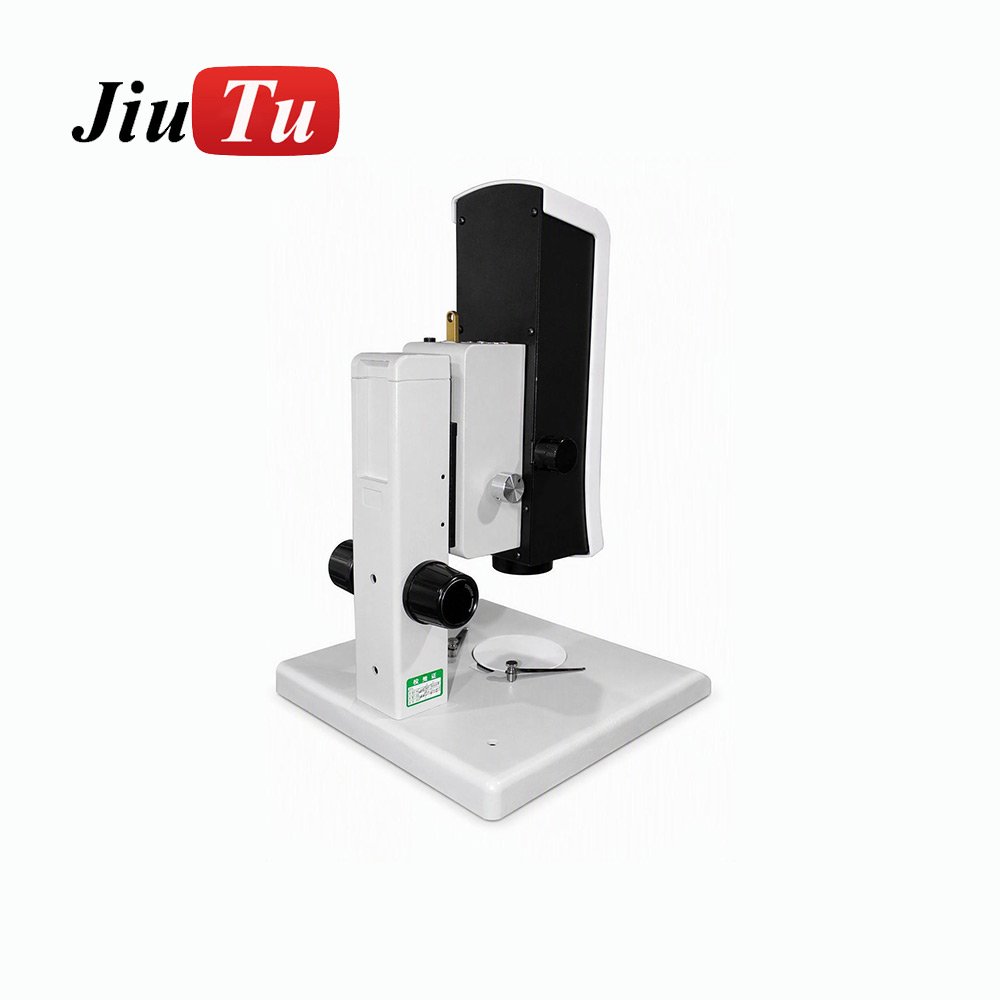
A useful bench test is simple: place the tallest regular assembly or fixture under the microscope, inspect both the center and edges of the board, then perform the same probe, tweezer or soldering-tool movement that an operator would use in production. Move the sample normally and watch for vibration, stand movement or difficulty returning to the inspection point.
Lighting should be tested by surface, not by brightness alone
A PCBA combines surfaces with very different reflection characteristics. Solder can create strong highlights, matte IC packages absorb more light, metallic connectors produce localized glare, and coatings or dark substrates can need different illumination to reveal surface detail.
The goal is not maximum brightness. It is enough contrast to see the required edge, residue, solder condition, scratch or surface feature without hiding useful information in glare or shadow.
Before approving a microscope, test at least one difficult reflective area and one low-contrast surface. If several material types are inspected regularly, record the useful lighting condition during qualification so operators do not have to rediscover the setup on every shift.
Do not qualify the workstation on one easy PCB. The most reflective solder joint, darkest component or lowest-contrast defect in the normal sample set often tells more about the usefulness of the lighting system than the cleanest demonstration image.
Decide What Must Happen After the Defect Is Found
A microscope for electronics quality control is also part of an information workflow. Before comparing camera features, decide who needs to see the image, whether evidence must be stored, and whether the operator is making only a visual judgement or also performing measurement.
Measurement tools are not automatically a metrology system. If a measured value will determine a formal accept/reject decision, verify the calibration method, accuracy, repeatability and any traceability requirements against the process tolerance.
When autofocus is actually useful
Autofocus becomes more valuable when operators move repeatedly between components or surfaces at different heights. In that situation, manual refocusing becomes part of every inspection cycle. It may add much less value when every sample is flat, fixed and examined on essentially one focal plane.
Test autofocus by moving across the real PCBA rather than keeping one object stationary. The relevant question is whether the focus behavior follows the operator’s normal inspection sequence without creating unnecessary pauses.
Capture should follow the QC record
Define the record before judging the capture feature. Does incoming inspection need one still image of a defect? Does process engineering need a short video? Does dimensional inspection need a saved measurement result? How will that file be associated with the lot, supplier, serial number or internal report?
A camera that can technically save an image is not automatically a good production solution. During qualification, run the complete sequence: locate the defect, focus, capture the image, perform any required measurement, save the result and retrieve it for review. The number of manual steps often determines whether the feature will actually be used consistently.
Where the SI-VMA fits
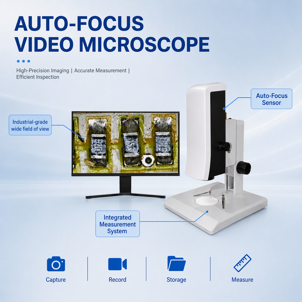
SI-VMA Automatic Focusing Video Microscope
The SI-VMA is worth evaluating when the inspection workflow benefits from screen-based viewing and when autofocus, recording or measurement removes a real manual step rather than simply adding another feature to the workstation.
- PCB, PCBA or FPC inspection with repeated movement between inspection points
- Large-screen review for operators, process engineers or quality teams
- Image or video documentation when inspection evidence must be retained
- Measurement workflows where dimensional checks form part of QC
- Applications where changing sample height makes focusing workflow important
Validate the Microscope With Real Samples Before Ordering
Specifications narrow the options, but representative samples should make the final decision. A short acceptance test can expose problems that are easy to miss on a datasheet: insufficient field of view, fixture interference, glare, slow navigation, unstable positioning, awkward recording or a focus workflow that becomes repetitive in production.
The sample set should represent the limits of normal work rather than only the average board. Include the smallest important defect, the tallest expected fixture or PCBA, a difficult reflective surface and a sample requiring capture or measurement when those functions matter.
- Begin with a normal working view. Confirm that the operator can find components, reference areas and inspection locations without excessive board movement.
- Move to the smallest critical defect. Increase magnification only until the required accept/reject judgement becomes clear.
- Install the tallest regular sample or fixture. Check focus, clearance and physical access at the same time.
- Challenge the lighting. Inspect reflective solder, dark components and the lowest-contrast defect available.
- Run the documentation sequence. Capture, measure if required, save the result and retrieve it in the same way planned for production.
- Repeat normal operator movement. Move between inspection points and sample heights while watching focus behavior, stability and handling.
Evidence of a good fit
The inspection loop feels natural
- Inspection areas are easy to locate at a wider view.
- The smallest critical defect is clear enough to judge.
- The real fixture fits with usable clearance.
- Difficult surfaces can be lit without uncontrolled glare.
- The stand remains stable during normal movement.
- Required records can be saved and retrieved efficiently.
Reason to reconfigure
The image works but the workflow does not
- High magnification looks clear but finding each target is slow.
- The real fixture fits only after removing required tooling.
- Hands or rework tools interfere with the viewing area.
- Reflective surfaces repeatedly lose detail in glare.
- The image moves excessively during normal bench work.
- Recording or measurement adds too many repeated steps.
When several microscope systems are being compared, use the same acceptance samples and the same inspection sequence for every system. Otherwise each demonstration can be optimized around a different ideal sample, making the purchasing comparison much less meaningful.
Common PCB Microscope Buying Mistakes
Most poor equipment choices are not caused by one obviously incorrect specification. They happen because one attractive specification dominates the decision while the rest of the workstation remains undefined.
- Buying maximum magnification. Maximum magnification does not show how quickly operators can find a target or whether additional enlargement reveals information that changes the QC decision.
- Testing only a bare PCB. Carriers, fixtures, sockets and tall components can consume the working space that appears generous during a simple demonstration.
- Using one easy lighting sample. A setting that looks excellent on a matte IC package may perform poorly on reflective solder or a low-contrast surface.
- Adding measurement by default. If the process only needs visual accept/reject decisions, advanced measurement functions may add complexity without improving the inspection result.
- Ignoring file handling. Capture becomes useful only when files can be saved, identified and retrieved in a way that fits supplier claims, traceability or internal reporting.
- Forgetting the display and bench layout. On a screen-based system, monitor size, position and viewing distance affect everyday use just as much as the camera output itself.
When does an upgraded inspection workflow make sense?
An upgrade is easier to justify when the current microscope creates a specific bottleneck. Operators may spend too much time refocusing between different component heights. Several people may need to review the same defect. Inspection photographs may require a separate camera, or measurement results may need to be transferred manually into another record.
In those situations, the useful question is not whether a new microscope has more features. It is whether a particular feature removes one of those known inspection steps.
There is less reason to pay for additional functions when inspection is occasional, the sample remains at one fixed focal plane and no image records or measurement data are required. The correct configuration is the one that solves the real QC task without adding unnecessary operating complexity.
If autofocus, large-screen review, image capture or measurement corresponds to a real inspection bottleneck, compare the SI-VMA against the same real PCB and acceptance samples. The product should earn its place by improving the inspection workflow rather than by offering the longest feature list.
Frequently Asked Questions
What microscope type is best for PCB quality control?
The best type depends on the inspection workflow. An eyepiece or stereo microscope can suit direct bench work and tool coordination, while a video microscope becomes more relevant when large-screen viewing, shared review, digital recording or on-screen measurement form part of the QC process. Compare them with the same representative PCB samples rather than choosing by microscope type alone.
How much magnification is useful for solder-joint inspection?
There is no single useful magnification for every solder joint. Use enough field of view to locate the joint efficiently, then increase magnification until the required visible condition can be judged confidently. The useful level depends on joint size, optics, camera output, display and lighting.
Why does working distance matter during PCB rework?
Rework requires physical access as well as visual access. Tweezers, probes, soldering tools and the operator’s hands need room around the assembly. A microscope can produce a clear image and still be unsuitable for rework if usable clearance is too limited.
Should a PCB microscope support image capture or measurement?
Choose these functions when the QC process actually needs them. Image capture can support traceability, supplier communication and defect records. Measurement becomes relevant when dimensional results must be documented. If measured values drive formal acceptance, verify calibration, accuracy and repeatability against the required tolerance.
Is a monitor included with the SI-VMA?
No. The external monitor is not included with the SI-VMA. Plan the display and its workstation position separately when configuring the inspection station.
Choose From Inspection Evidence, Not a Single Specification
The strongest way to select an industrial microscope for PCB quality control is to treat it as a complete inspection workstation rather than a magnification purchase. Begin with the smallest critical defect, verify the field of view needed to find it, then test useful magnification, working distance, lighting, stand stability and the documentation process using representative PCB or PCBA samples.
This also makes purchasing discussions more useful. Instead of asking a supplier which microscope is “best,” provide the physical and workflow conditions the system must satisfy. The proposed configuration can then be judged against the same repeatable acceptance test.
Application & Configuration Review
Prepare the Real PCB Inspection Requirements Before Finalizing the Microscope
For a useful configuration review, prepare the information that changes the real inspection workstation:
- PCB, PCBA or sample dimensions
- Maximum component or fixture height
- Smallest defect or feature to inspect
- Surface material and reflection conditions
- Visual inspection or measurement requirement
- HDMI viewing and recording requirement
- Required voltage
- Destination and installation conditions
With those details, the configuration discussion can focus on usable field of view, working clearance, lighting, focusing behavior and the inspection-record workflow instead of selecting a microscope from one headline specification.